PCB Design Ltd
introduces
Design challenges of PCIe Gen4
using Altium
Date: 16.02.2023. (Thursday)
14.00 GMT – (15.00 CET)
Duration: 1 hour
Major topics:
- PCIe Gen 4 SI simulation and measurements
- Stackup and material selection
- Practical layout guidance
- Optimal routing
- Effect of back-drill
- Anti-pad design
- Powering 50+A core voltage
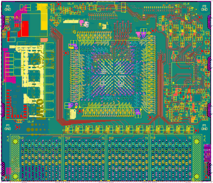
In this presentation, we present a detailed analysis of a state-of-the-art 16-layer, 128-lane Gen 4 PCIe design using Altium PCB design Tools.
The first part of the presentation focuses on the simulation and measurements of the PCIe Gen 4 signal integrity. This includes a thorough examination of the design’s compliance with the standard, as well as an analysis of the design’s performance under different operating conditions. The simulation results are then validated through measurements on the actual hardware, providing a comprehensive evaluation of the design’s signal integrity.
The second part of the presentation examines the stackup and material selection used in the design. The stackup is the arrangement of the different layers in the design and it is critical to ensure that the signal integrity is not compromised. We discuss the different types of materials used, their electrical properties and how these choices impact signal integrity and performance.
In the third part of the presentation, we provide valuable practical guidance for layout engineers. We provide insights on optimal routing strategies to minimize signal loss and crosstalk. One of the key challenges in high-speed signal integrity is the routing of the signals. We discuss how to use different routing techniques such as differential pairs, matched lengths, and controlled impedance to minimize signal loss and crosstalk.
We also explore the effect of backdrill on signal integrity. Backdrill is a technique used to remove the copper from the backside of a PCB to reduce the parasitic capacitance and improve signal integrity. We discuss how backdrill can be used to improve the performance of the design and the trade-offs involved.
Another important aspect of the design is anti-pad design. Anti-pads are used to reduce the capacitance between the signal and the power/ground planes. We discuss how to use anti-pads to improve the signal integrity and how to design them for optimal performance.
Finally, we provide guidance on powering the high current requirements of the 50+ A core voltage. Powering the high-speed circuits in a design is a critical aspect that is often overlooked. We discuss the different types of power distribution networks, and how to design them for optimal performance.
Overall, this presentation will present a comprehensive analysis of a cutting-edge Gen 4 PCIe design, and provides valuable insights for engineers working on similar projects.
The information presented will be useful for those looking to improve the signal integrity and performance of their own PCIe designs. The detailed analysis and practical guidance provided in this paper will help engineers understand the complexities of high-speed signal integrity and how to design a robust and reliable PCIe design.
